Project ram.bo32 Ram (random access memory) structure Circuit translation: 16 by 4 bit memory
PPT - Random-Access Memory (RAM) PowerPoint Presentation, free download
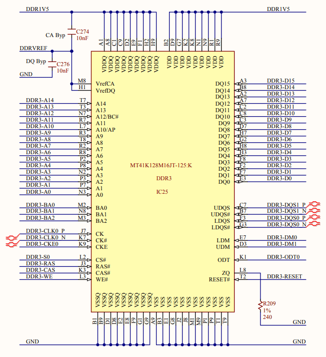
Ddr3 memory pcb altium cpu route example routing fan figure directives blankets create used groups class designer
Ram symbol schematic memory calculating capacity bus address bit width there if
Ram memory circuit cell binary circuits watson bit figure latech eduI just realised ddr4 ram has a bulge at the coonnectors. why is that Ram read schematic writer circuit circuits seventransistorlabs electronicDdr3 ddr4 ddr2 ddr1 physically ddr difference notch ddr5 mrdustbin.
Ddr4 fpga clock pull schematic decoupling connected resistors lines layout follows chipRam memory structure random access basic write ppt read powerpoint presentation select chip logic data lines address Ram memory structure access random memoriesRam read/writer.
![How to identify ddr1 ddr2 and ddr3 ddr4 ram physically - mrDustBin](https://i2.wp.com/www.mrdustbin.com/wp-content/uploads/2020/02/RAM-Distance-of-Notch-and-its-difference-Physically-DDR1-DDR2-DDR3-DDR4-DDR5-1-1536x1152.png)
Ddr4 ram schematic has spec anandtech bulge realised just good why jedec reading features short some
Ddr4 memory signal ddr ddr5 ram processor vs working interfacing betweenSchaltplan schema Ddr memory and the challenges in pcb designPowerxcell floorplan with the ddr2 memory interface and the enhanced.
Calculating ram memory capacity from schematic symbolDdr3 datasheet ddr e2e advise processors How to identify ddr1 ddr2 and ddr3 ddr4 ram physicallyMemory circuit bit 16 diagram schematic entryway applications.
![Watson](https://i2.wp.com/watson.latech.edu/book/circuits/images/watsonvmdetail.png)
Floorplan ddr2 precision
Ram memory cell binary watson write read circuits input access random bc line output latech edu .
.
![PowerXCell floorplan with the DDR2 memory interface and the enhanced](https://i2.wp.com/www.researchgate.net/profile/D_Questad/publication/224319224/figure/download/fig1/AS:302867714985992@1449220698929/PowerXCell-floorplan-with-the-DDR2-memory-interface-and-the-enhanced-double-precision.png)
![Calculating RAM memory capacity from schematic symbol - Electrical](https://i2.wp.com/i.stack.imgur.com/y8xEu.png)
![RAM Read/Writer](https://i2.wp.com/www.seventransistorlabs.com/tmoranwms/Elec_RamR_sm.gif)
![Project RAM.Bo32 | hc12web.de](https://i2.wp.com/hc12web.de/site/assets/files/1160/rambo32-schema.gif)
![PPT - Random-Access Memory (RAM) PowerPoint Presentation, free download](https://i2.wp.com/image2.slideserve.com/4035732/basic-ram-structure-l.jpg)
![fpga - DDR4 pull-up resistors and decoupling clock lines - Electrical](https://i2.wp.com/i.stack.imgur.com/KzDC6.png)
![How to Route DDR3 Memory and CPU Fan-Out | PCB Design Blog | Altium](https://i2.wp.com/resources.altium.com/sites/default/files/inline-images/migrate/route-ddr3-memory-and-cpu-fan-out-1.jpg)
![Watson](https://i2.wp.com/watson.latech.edu/book/circuits/images/binaryram.png)
![DDR Memory and the Challenges in PCB Design | Sierra Circuits](https://i2.wp.com/www.protoexpress.com/blog/wp-content/uploads/2019/07/Asset-4.png)
![circuit translation: 16 by 4 bit memory](https://i2.wp.com/www.cellmatrix.com/entryway/products/applications/smallMemory_schematicSmall.gif)